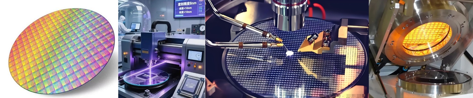
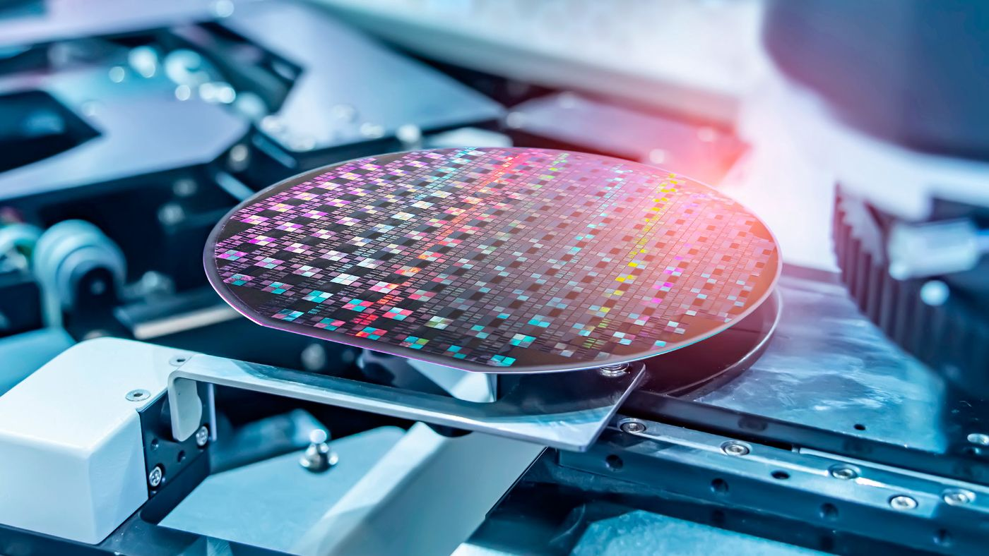
On the fab floor, temperature isn’t a knob you turn—it’s a spec you live by. A 0.5°C drift will shift a line width. A particle from a heater can kill a die. In semiconductor machinery, the thermal module quietly decides yield, uptime, and cost per wafer. We design thermal systems around the process window, not the panel. The target is wafer-level uniformity of ±0.1°C, and we get there with NIR radiant heating, quartz windows, and closed-loop pyrometry that controls temperature at the surface—not somewhere in the bulk. It runs in Class 1–100 cleanrooms, with zero particle generation verified by in-line monitoring. Every bake—soft bake to pull out solvent, hard bake to lock in adhesion—repeats within a tight thermal budget. Reliability over 24 hours comes from redundant sensing and a thermal architecture that holds setpoint through line voltage swings and ambient drift. Lithography clusters need thermal repeatability across tools and shifts. Our module delivers consistent photoresist bake profiles, which cuts CD variation and trims shot count. That means fewer rework lots, less scrap, and throughput that stays steady. Energy use comes down because NIR heats directly, ramping fast with minimal idle mass. In high-mix fabs, the same platform handles multiple wafer sizes and recipes without requalification, which simplifies the spares strategy across the supply chain. Integration is not trivial. The unit needs a dedicated power feed, EMI-clean cabling, and a cleanroom-rated exhaust to keep particle discipline intact. Plan a short commissioning window to align the pyrometer calibration with your recipes. Once it’s in, the trade is straightforward: you accept a tighter mechanical envelope for a wider process margin, fewer excursions, and uptime you can plan around.