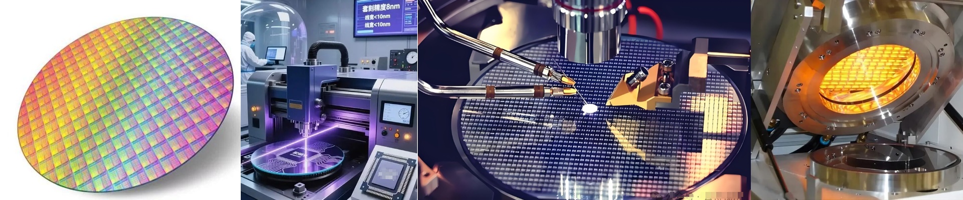


We Test Every Single Sensor. No Exceptions.
In the world of wafer fab, one tiny electrical leak is all it takes to scrap an entire batch of silicon. That’s a nightmare nobody wants. That’s why we don’t do “batch sampling.” We don’t just test a few units and hope for the best. Every single lamp and sensor that leaves our shop goes through 100% withstand voltage (Hipot) and insulation resistance testing. Every. Single. One.
The reality of dielectric breakdown
Wafer tools are tight. You’ve got high-voltage heating elements sitting right next to incredibly sensitive semiconductor substrates. In that environment, your insulation has to be perfect. To make sure it is, we push the voltage way past the normal operating specs. We’re looking for the stuff you can’t see—tiny pinholes in the quartz or a slight degradation in the ceramic. If we see a leak of even a few milliamps? It goes in the trash.
Why we can’t just “sample”
Random sampling is a gamble, and high-precision tools aren’t the place to bet. Think about a hairline fracture in the insulation. It’s invisible. But once it’s in your tool, it can arc. That creates electrical noise or a direct short that trips your safety interlocks and shuts everything down. By testing every unit, we make sure that the insulation is rock solid from the moment it leaves our bench until it’s installed in your cleanroom.
The trade-off: Power vs. Space
Here’s the thing: if you need extreme insulation resistance, you usually need more material. That means thicker ceramic housings or specialized coatings. It makes the sensor bulkier. You’ll have to balance that extra size against the space you have in your tool. If you’re spec-ing a sensor for heavy-duty voltage isolation, just double-check that your mounting brackets have the room to handle the extra girth. When your order arrives, you’ll get the test reports for every serial number. You can wire them in and get to work, knowing the insulation isn’t going to blow out the moment you put it under load.